Precision-engineered printed circuit boards that power the next generation of electronic devices. From concept to production, we deliver excellence.
25+ Years of Excellence
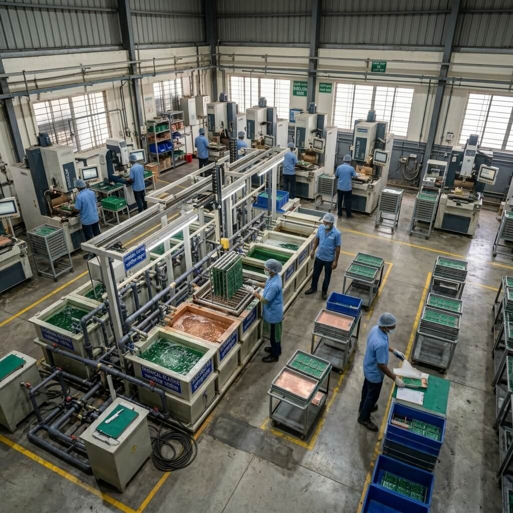
Advanced PCB Fabrication Facility
Designed & Delivered for Innovation
PCB fabrication is the foundation of every electronic breakthrough. Whether based on your submitted designs or engineered by our in-house experts, we transform concepts into high-performance printed circuit boards with absolute precision, consistency, and care.
100% Design Adherence
Every PCB is manufactured in our state-of-the-art facility and validated through rigorous quality checks to ensure exact compliance with your design intent.
Agile & Scalable Manufacturing
With capabilities up to 24-layer PCBs, we support rapid prototyping, small batches, and large-volume production—delivering consistently high quality with short lead times.
Powering Innovation Across Multiple Industries
Our high-quality PCB fabrication solutions are trusted by innovators, institutions, and enterprises across a wide range of industries that demand performance, reliability, and scalability.
Research & Development
Aerospace
Defence
Students & Hobbyists
Renewable Energy
Educational Institutes
Automotive
Industrial Electronics
Railways
Test, Measurement & Metering
Proto PCB Fabrication That Unlocks Efficiency
Designed for speed, flexibility, and cost control, our proto PCB services help you prototype, validate, and innovate without barriers.
Transparent Pricing
Know your exact PCB cost upfront with our easy-to-use online price calculator—no surprises.
MOQ: Just 5 Unit
Order exactly what you need—from a single prototype to multiple iterations—without restrictions.
No Setup Charges
Our streamlined fabrication process removes extra setup costs for prototypes—making prototyping affordable.
Fast Turnaround
Get your prototype PCBs delivered in as little as 3 working days.
Our End-to-End PCB Fabrication Process
From design validation to final testing, we ensure every PCB meets the highest standards of quality and reliability through our comprehensive manufacturing process.
Design & Engineering Review
Our engineering team validates your design files for manufacturability, performing DFM checks to identify potential issues before production begins.
Material Selection & Preparation
We source high-quality substrates (FR-4, Rogers, Aluminum) and copper-clad laminates, precisely cut to your PCB dimensions with strict material traceability.
Precision Imaging & Etching
Using advanced LDI technology, we transfer circuit patterns onto copper layers with micron-level accuracy, followed by precise etching to create the circuit traces.
Multi-Layer Lamination
For multi-layer boards, we use high-pressure hydraulic presses to bond layers together with prepreg, ensuring perfect alignment and reliable interlayer connections.
Drilling & Plating
High-precision CNC machines drill micro-vias and through-holes, followed by electroless and electrolytic copper plating to establish conductive pathways between layers.
Quality Control & Testing
Every PCB undergoes rigorous electrical testing, AOI inspection, and impedance verification to ensure 100% functionality before shipment.