Complete PCB Design Files
Guide
Everything you need to know about preparing files for PCB fabrication and assembly. Ensure smooth manufacturing by providing complete and accurate design files.
1 Schematic File
Key Purpose
Schematics are essential for verifying design logic, ensuring proper connectivity, and serving as a reference during troubleshooting and debugging phases.
What to include:
- All electrical symbols and their connections
- Component designators (R1, C1, U1, etc.)
- Net names for critical signals
- Power and ground connections clearly marked
- Test points and measurement indicators
2 Bill of Materials (BOM)
The Bill of Materials is a comprehensive list of every component required to assemble your PCB. An accurate and complete BOM ensures correct component sourcing, faster production, and prevents assembly errors that could lead to costly rework.
Preferred Formats
Submit your BOM in CSV, Excel (.xlsx), or PDF format with clearly labeled columns for each required field.
Essential BOM Columns:
- Quantity: Number of each component needed
- Reference Designator: Component identifier (R1, C1, U1)
- Value & Footprint: Component specifications and package type
- Manufacturer Part Number: Exact MPN for sourcing
- Description: Clear component description
- Supplier: Preferred vendor (optional but helpful)
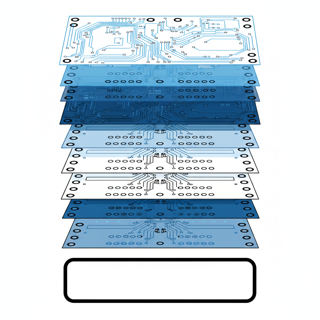
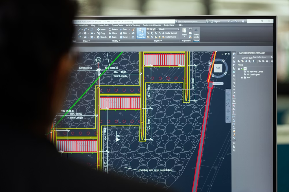
3 Gerber Files – Core of Fabrication
Gerber files are the universal standard for PCB manufacturing. They contain the exact blueprint of your PCB, defining each physical layer including copper traces, solder mask, silkscreen, drill holes, and board outline. Without properly generated Gerber files, fabrication is not possible.
Critical Check
Always use Gerber viewers to verify your files before submission. Ensure all layers align correctly and there are no design rule violations.
Required Gerber Layers:
- Top & Bottom Copper Layers (.GTL, .GBL)
- Solder Mask Layers (.GTS, .GBS)
- Silkscreen Layers (.GTO, .GBO)
- Drill Files (Excellon format .DRL, .TXT)
- Mechanical / Outline Layer (.GML, .GKO)
- Board Outline with cutouts and slots
- Paste Mask Layers (for solder paste application)
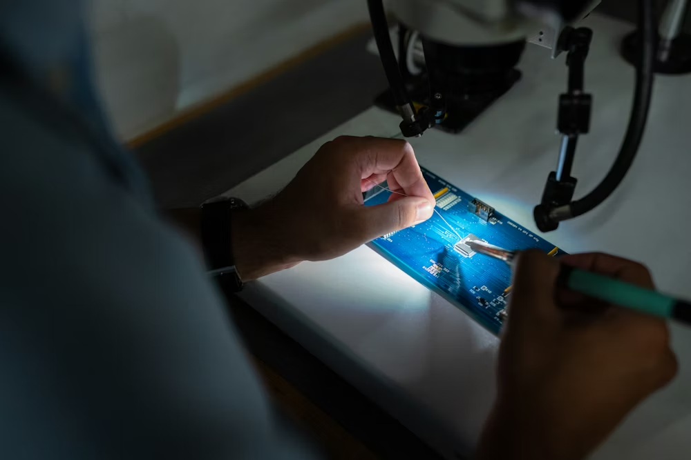
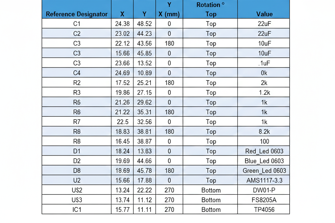
4 Pick & Place File (PnP)
The Pick & Place file provides machine-readable data that helps automated assembly equipment accurately position components on the PCB.
Machine Compatibility
Most assembly machines accept CSV or TXT formats with X/Y coordinates relative to a defined board origin (usually bottom-left corner).
Required PnP Data Columns:
- Reference Designator: Component identifier (R1, C1, U1)
- X/Y Coordinates: Position relative to board origin (in mm or inches)
- Rotation Angle: Component orientation in degrees (0-360)
- Top or Bottom Side: Placement side designation
- Component Value: Resistance, capacitance, part number, etc.
- Footprint Name: Package type (0805, SOIC-8, QFN-48, etc.)
Why Are These Files So Important?
Avoid Manufacturing Delays
Incomplete or incorrect files are the #1 cause of PCB manufacturing delays. Each missing file can add 2-5 business days to your turnaround time.
Ensure Design Accuracy
Complete files allow manufacturers to run thorough design rule checks (DRC) and manufacturability analysis, catching potential issues early.
Faster Turnaround
Complete and properly formatted files enable automated processing, reducing manual handling and speeding up both fabrication and assembly stages.
Higher Quality & Reliability
Accurate files ensure components are correctly placed, soldered, and aligned, resulting in higher first-pass yield and more reliable final products.
Providing complete and properly formatted design files is the single most effective way to guarantee faster turnaround, higher reliability, and better overall PCB quality. Missing or incorrect data can cause alignment issues, assembly errors, or even complete board failure.
Ready to Submit Your PCB Design?
Upload all required files through our secure portal. Our engineering team will review your design and provide feedback within 24 hours.
Need Help Preparing Your Files?
Our engineering support team is available to help you prepare and verify your design files. Contact us for a free design review before submission.
PCB Manufacturing Guide
A comprehensive resource for preparing PCB design files for fabrication and assembly. Follow these guidelines to ensure successful manufacturing of your printed circuit boards.